
Core i9-12900K processor review: a revolution in the mind
Core i9-12900K processor review: a revolution in the mind
Contents
show
The processor that will change everything – something like this can be characterized by Intel’s enthusiasm, which accompanied the release of Alder Lake. A year and a half ago, Raja Koduri spoke about Alder Lake in the vein that this is the most significant step for Intel since the introduction of Core processors in 2006. And it’s hard to disagree with that. A detailed article on the Alder Lake architecture was recently published on our website, and from the facts presented in it it really follows that now we can expect almost a seismic shift in the market, at least in the segment of processors for personal computers.
Work on Alder Lake began around the time AMD began to make its first notable breakthroughs with its Zen products, and as such, it can be seen as Intel’s answer to the changing rules of the game in the processor market. That is, all previous Comet Lake and Rocket Lake that Intel released as opposed to successive generations of Ryzen were more likely to move by inertia. But now, Intel has finally woken up and moved to action. But the fact that the release of Alder Lake should mark a new round of the processor race, in which AMD’s leadership will be called into question, is just one of the reasons why so much attention is riveted to Intel’s new product.
The second reason is that whether Alder Lake is better than Zen 3 or not, it’s still a revolution. Koduri was right: we have not seen such large-scale updates for a very long time. Alder Lake has significantly increased the number of cores, finally introduced a truly fresh process technology, applied a hybrid architecture that combines two heterogeneous types of cores, and also added Thread Director technology, thanks to which the processor was able to directly interact with the operating system scheduler. In other words, today, on the day the sale of Alder Lake processors for desktop computers begins, there are many topics for conversation. Therefore, we will not beat around the bush, but immediately get to the point – to a detailed acquaintance with the new generation of Intel’s flagship processor, the Core i9-12900K.
⇡#What is Alder Lake: characteristics and lineup
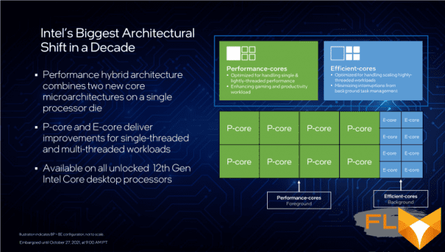
The main and most interesting feature of Alder Lake is hybridity. Intel decided to try a fundamentally new approach in the design of desktop processors and refused to create processors based on the same type of cores. The current concept suggests that different tools should be used for different purposes, and Alder Lake has found use in two different microarchitectures in terms of their properties – productive and energy efficient.
Although this is a completely fresh idea for desktop solutions, in general, processors consisting of different types of cores are hard to surprise anyone these days. The big.LITTLE approach has long been used in mobile chips, and there the coexistence of heterogeneous cores does not lead to any negative consequences. Moreover, Intel itself managed to experiment with a hybrid design, releasing an ultra-mobile Lakefield processor in the middle of last year, made up of one productive and four energy-efficient cores. Devices based on it have demonstrated quite convincingly the feasibility of such a design for personal computers, and now Alder Lake is expanding the scope of this concept.
However, if hybridity in itself does not appeal to you at all, Alder Lake still deserves to be paid attention to. One of the microarchitectures around which the new processor is built is Golden Cove, and it is able to “pull” this entire project on its own, without any additions. Thanks to it, at least half of Alder Lake cores promise a 19% increase in specific performance compared to Rocket Lake cores, and this alone is enough to make new Intel solutions interesting, at least for gamers.
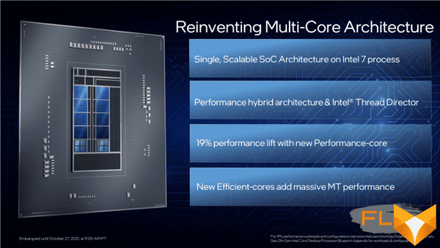
In total, there are two types of cores in Alder Lake: productive P-cores on the Golden Cove microarchitecture and energy-efficient E-cores on the Gracemont microarchitecture. They were developed independently of each other, and when they were created, the engineers faced fundamentally different tasks. Golden Cove are wide and large cores that are optimized for peak single-threaded performance. At the same time, Gracemont is focused on simplicity and energy efficiency. The logic of combining Golden Cove and Gracemont in one processor is that background tasks that do not require maximum execution speed can be serviced by E-cores with minimal energy costs. At the same time, P-cores are needed mainly for front-end applications that are not tied to waiting for data to arrive and need to be executed as quickly as possible. And if it comes to the need to execute multi-threaded resource-intensive tasks, then to service them in a hybrid processor, you can immediately connect all available capacities – both P-cores and E-cores.
Today, Intel begins selling the first batch of members of the Alder Lake family. It includes six models of overclocking Core 12th generation, related to the Core i9, Core i7 and Core i5 series. The number of cores that these processors offer is from 10 to 16, they all support DDR5, PCI Express 5.0, new overclocking options, and they all have completely new thermal parameters. Moreover, at this stage, Intel changed the meaning of other quantities appearing in the specifications: a hybrid design requires a different look even at the usual passport characteristics.
Please note that the specification table below contains separate information about different types of cores, but at the same time general information about the size of the cache memory and thermal characteristics.
| Number of cores | Number of threads | P-core frequency, GHz | E-core frequency, GHz | L3 cache, MB | Graphics | Basic TDP, W | Turbo TDP, W | Price | |
|---|---|---|---|---|---|---|---|---|---|
| i9-12900K | 8P + 8E | 24 | 3.2-5.2 | 2.4-3.9 | 30 | UHD 770 | 125 | 241 | $589 |
| i9-12900KF | 8P + 8E | 24 | 3.2-5.2 | 2.4-3.9 | 30 | No | 125 | 241 | $564 |
| i7-12700K | 8P + 4E | 20 | 3.6-5.0 | 2.7-3.8 | 25 | UHD 770 | 125 | 190 | $409 |
| i7-12700KF | 8P + 4E | 20 | 3.6-5.0 | 2.7-3.8 | 25 | No | 125 | 190 | $384 |
| i5-12600K | 6P + 4E | 16 | 3.7-4.9 | 2.8-3.6 | 20 | UHD 770 | 125 | 150 | $289 |
| i5-12600KF | 6P + 4E | 16 | 3.7-4.9 | 2.8-3.6 | 20 | No | 125 | 150 | $264 |
The explanation here is pretty simple. Intel doesn’t want new processors to be classified by the total number of processing cores, so the number of P-cores and E-cores is always listed separately. The same Core i9-12900K still cannot be considered a full-fledged 16-core, at least because its E-cores do not support Hyper-Threading and operate at much lower clock speeds. And the idea of hybrid design is that P-cores, E-cores and virtual cores served by Hyper-Threading technology have different purposes, although they can, if necessary, take on parallel multi-threaded workloads together.
The list of processors, sales of which begin today, includes six models. The launch of the new generation of Core began from the top down. At first, the company plans to start selling overclocking flagships, and simpler models will come to the market later, when the first users from among enthusiasts will already appreciate the delights of the new design and hybrid architecture.
The presented Alder Lake differ among themselves in the number of P- and E-cores, in clock speeds and in the amount of cache memory of the third level. That is, the main differentiating factors remained generally the same as before. The older models belonging to the Core i9 series received eight productive and energy-efficient cores each. In Core i7 processors with eight performance cores, four power-efficient cores side by side. And in Core i5 processors, the number of productive cores is reduced to six. All this means that the number of P-cores in the Core i9 / i7 / i5 series has not changed compared to the Rocket Lake processors (although these cores themselves have changed), but in addition to them, the new Alder Lake received eight or four energy-efficient cores.
At the same time, all representatives of the 12th generation Core announced today have the same set of 16 PCIe 5.0 lanes and 4 PCIe 4.0 lanes, as well as support for DDR5-4800 and DDR4-3200 memory. And models without the letter F in the name are also equipped with an integrated UHD Graphics 770 Xe-LP class graphics core with 32 execution units, functionally similar to the integrated UHD Graphics 750 graphics from Rocket Lake processors.
As for the recommended prices of new products, they seem quite democratic: the older processor costs $589, which is only $50 more expensive than the Core i9-11900K. And the option without the Core i9-12900KF graphics core with a recommended price of $564 can easily be opposed to the 12-core Ryzen 9 5900X. But such positioning is typical only for the older model in the series. The mid-range i7-12700KF is priced significantly cheaper by Intel than the eight-core Ryzen 7 5800X, while the younger Core i5-12600KF is more affordable than the six-core Ryzen 5 5600X. However, the Core i7-12700K and Core i5-12600K are $10 and $27 more expensive than the older processors of the same series, but of the previous generation.
Comparing Alder Lake with desktop processors based on the Zen 3 microarchitecture in terms of any other characteristics, except for prices, hardly makes sense – these design proposals are very different. But still, we note that Intel now wins not only in terms of clock speeds, but also in terms of the total number of cores. However, Alder Lake continues to be inferior to the competitor’s offerings in terms of L3 cache capacity and heat dissipation, especially if you are guided by a more honest parameter of not the base, but the turbo TDP.
⇡#Where did the “typical heat release” go
Previously, in the specifications of processors, Intel indicated for its chips the amount of calculated heat dissipation – TDP, which was usually equal to 65, 95 or 125 watts. From a formal point of view, the definition of TDP sounded like the maximum heat dissipation of the processor at the base frequency, but in fact this value was supposed to limit the consumption of the processor during continuous loads.
However, in the case of Intel processors of the latest generations, TDP has practically lost any practical significance. The problem is that trying to keep the processor’s heat dissipation within the TDP set by Intel leads to a catastrophic drop in performance. Therefore, in real systems, completely different consumption limits are used everywhere, and in the configurations that enthusiasts assemble, they are completely canceled altogether. For some time, Intel still tried to deal with this situation by formalizing the requirements for processor consumption through the values PL1 and PL2 (maximum consumption for long-term and short-term load). But with the release of Alder Lake, the company came to the realization that it was necessary to completely change the approach to declaring heat dissipation.
The data sheets for the 12th generation Core family now have two different values that describe their heat dissipation and power consumption. The first, Processor Base Power (PBP), is the maximum heat dissipation at the base frequency, that is, an analogue of the old TDP. And the second, Maximum Turbo Power (MTP), is the honest maximum heat dissipation that a processor can achieve in turbo mode. Thus, Intel’s thermal and power performance policy becomes more honest.
It is logical to assume that Maximum Turbo Power is a new name for PL2: maximum consumption during short-term loads, while Processor Base Power is the long-term consumption limit of PL1. But this will be true only for non-overclocker processors, which will be announced later. The same six Alder Lake models that are released now have no restrictions on long-term consumption at all. They can operate within the Maximum Turbo Power value at any time intervals. And in the old terminology, this means that PL1 = PL2 = MTP.
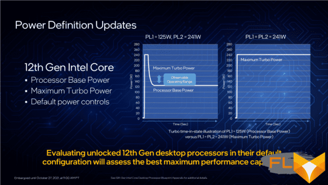
In other words, Intel has officially recognized what has become the de facto standard for a long time. The consumption and heat dissipation of overclocking processors should not be constrained by any additional limits, and therefore, the Core i9 is now officially allowed to dissipate 241W of heat on a permanent basis, the Core i7 – 190W, and the Core i5 – 150W. In this case, motherboard manufacturers, most likely, will not take MTP values into account at all. For example, in those LGA1700 boards that we got acquainted with when preparing this material, any artificial consumption limits for Alder Lake were completely canceled.
⇡#Introduction to Semiconductor Crystal
Intel plans to use two varieties of semiconductor chips for the Alder Lake family of desktop processors. The large one is C0 stepping with eight P-cores and eight E-cores, and the small one is H0 stepping with six P-cores and no E-cores at all. The models presented at the moment are based exclusively on large chips, small versions of silicon are planned to be introduced with the release of the younger representatives of the Core i5 and Core i3 series.
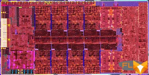
Although we used the adjective “big” to describe the size of an Alder Lake die in the paragraph above, in reality, even its 16-core modification does not look monstrous. Intel has finally shifted its desktop processor production to the modern Intel 7 (10 nm Enhanced SuperFin) process technology, which immediately reduced the die area. The older version of Alder Lake silicon occupies only 210 mm 2, and this is almost a quarter less than the area of \u200b\u200bthe eight-core Rocket Lake die. As a result, in terms of the size of the semiconductor crystal, the 16-core Alder Lake is comparable to the 10-core Comet Lake on much simpler Skylake cores and with less cache memory.
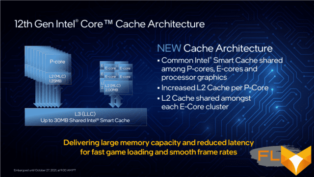
While the Comet Lake and Rocket Lake cores had 256 and 512 KB of L2 cache, the Alder Lake P-cores received 1.25 MB of L2 cache per core. As for the E-cores, they are grouped into clusters of four with a common 2 MB L2 cache, which is divided into all four cores at once. As for the top-level cache, its size in Alder Lake reaches 30 MB, while in processors of previous generations the L3 cache did not exceed 20 or 16 MB, respectively. As a result, the total amount of cache memory of the new Intel processors reaches 44 MB, which exceeds even the total amount of cache memory of AMD single-chip processors with the Zen 3 microarchitecture.
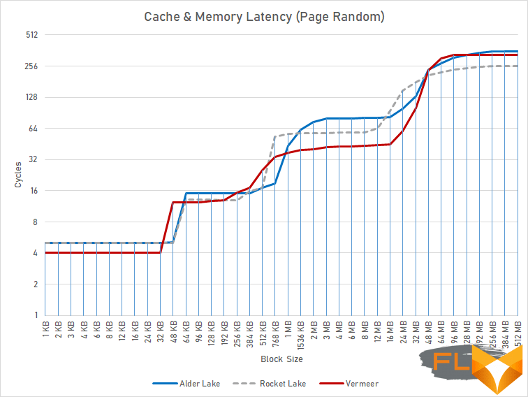
However, the increase in cache volumes in Alder Lake had a negative impact on their latency. Compared to Rocket Lake, the latency of the L2 cache has increased from 13 to 15 cycles, and the L3 cache has increased from 58 to about 80 cycles. The latter indicator, by the way, almost doubles the latency of the L3 cache of processors with the Zen 3 microarchitecture. In other words, although the L3 cache in Alder Lake is large, it is now comparatively slow.
Familiarity with the image of the Alder Lake semiconductor crystal allows us to draw other interesting conclusions. For example, that the assumption of the same size of one Golden Cove core and a quad-core Gracemont cluster turned out to be wrong in the end. In reality, four E-cores take up about 25% more space on the Alder Lake die. You can also pay attention to the fact that the UHD Graphics 770 graphics core began to take up quite a bit of space on the chip – only 16% of the silicon area is spent on it.
Alder Lake still uses a bidirectional ring bus to link all functional blocks together, but not all cores have equal access to it. While each of the P-cores has direct access to this bus, which runs along the center of the chip, clustered E-cores work with it in a different way. Here, four E-cores have only one bus access port, and the clustered cores themselves communicate with each other by exchanging data through a common L2 cache. All this leads to the fact that the delays of inter-core data transfers in Alder Lake are not uniform.
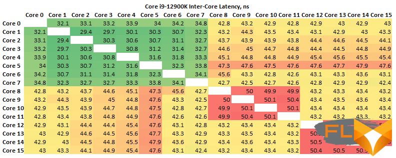
Only P-cores can exchange with each other at maximum speed. They manage to do this even faster than the cores in Rocket Lake processors. But when it becomes necessary to exchange information between the P- and E-cores, the waiting time immediately increases by 37%. Data transfers between E-cores that belong to different clusters have approximately the same latency. But the transfer of data between the nearest E-cores within the same cluster is an even more painful process. However, the maximum inter-core exchange latency observed in Alder Lake at the level of 50 ns is still better than the delay that occurs in Ryzen processors when transferring data between cores located in different chiplets.
⇡#Thread Director: how it works in OS
One of the main doubts that arise when discussing Alder Lake hybrid processors concerns whether modern operating systems will be able to properly dispose of an array of heterogeneous computing cores. Although in general the problem of distributing threads across different cores has existed for a long time and, for example, in the case of virtual cores created as part of Hyper-Threading technology, it is successfully solved, with Alder Lake everything is noticeably more complicated. Now the operating system scheduler must think not only about maximizing performance, but also about energy efficiency, trying to take advantage of the E-cores.
Intel says it took close collaboration with Microsoft to figure out the right algorithms for using Alder Lake resources, resulting in the Windows 11 operating system scheduler getting all the necessary improvements. At a lower level, this means that Windows 11 is trained to work with a custom microcontroller built into Alder Lake processors.
This microcontroller is the essence of Thread Director technology. It continuously collects information about the thermal and energy parameters of the cores and analyzes the instruction stream executed by each core, transferring the results of this analysis to the operating system. This mechanism is used by the Windows 11 scheduler – in this OS, the distribution of threads among the cores occurs taking into account the feedback implemented through the Thread Director. Alder Lake should work better in Windows 11 because of the feedback – in this operating system, E-cores can really be used to service background threads that do not need high performance. At the same time, in Windows 10, where feedback from the Thread Director is not implemented, Alder Lake processors will obviously perform worse in terms of energy efficiency in the first place. In the previous version of the operating system, the scheduler is also able to take into account information about differences in the performance of different cores, but interactive analysis of the instructions they execute, as well as an assessment of their current load and efficiency, is not available to it.
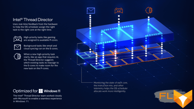
As Intel explains, the main purpose of Thread Director is to sort active threads into different classes for the operating system scheduler: normal; those that use AVX instructions; and those that do not need high performance (whose work, for example, is limited by the influx of external data). To determine the types of threads in the Thread Director, a special, pre-trained AI algorithm is used, which is precisely based on the telemetry data collected by the microcontroller. Further, the Thread Director will recommend that ordinary and AVX threads be executed on P-cores, while he will suggest sending threads waiting for data to be sent to E-cores. All this information is passed to the Windows 11 scheduler, and he can either use it directly, or adjust these recommendations in accordance with which tasks the user has set for himself in the foreground and which have been turned off.
⇡#New DDR5 memory
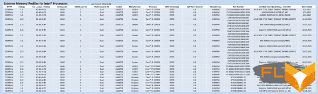
A big innovation in Alder Lake processors that deserves a separate story is a new memory controller that supports not only DDR4, but also DDR5 SDRAM. Formally, Intel says in the specifications about compatibility with DDR5-4800, but in fact the new processors are able to work with faster modules. Thus, memory manufacturers have already announced modules with DDR5-5200, DDR5-5600, DDR5-6000, DDR5-6400 and even DDR5-6800 frequencies. And all these options are quite compatible with the new processors. Intel recently published a list of Alder Lake tested DDR5 SDRAM modules, and it includes modules with speeds exceeding those stated in the specifications.
To support a wide range of DDR4 and DDR5 memory speeds, the controller in Alder Lake received three dividers at once, which determine different ratios between the frequencies of the memory controller and the modules themselves: Gear 1, Gear 2 and Gear 4. In the first case, the memory works with the controller at synchronous frequencies , in the second, the memory frequency doubles, and in the third, the memory frequency increases relative to the controller frequency by four times. This scheme is similar to how the memory was built in Rocket Lake processors, but now there are more dividers.
Since the frequencies of DDR5 modules start at a rather high mark of 4400 MHz (which is higher than the maximum JEDEC-certified DDR4 frequency), the Gear 1 mode is not applicable with them, it is left exclusively for DDR4 SDRAM. But in the gear 2 frequency doubling mode with Alder Lake, any overclocker DDR5 SDRAM modules work fine. The Gear 4 mode is also functional, but it makes no sense to use it yet – it imposes a higher penalty on the performance of the memory subsystem compared to Gear 2.
By themselves, DDR5 SDRAM modules, although they have the same 288 pins as DDR4, are electrically and mechanically incompatible. Installing DDR5 modules (and vice versa) in DIMM slots intended for DDR4 SDRAM will not work – a different location of the key cutout will interfere. The use of connectors of different types is not a whim of developers, DDR5 memory is fundamentally different from the previous standard. Its increased frequencies are not due to overclocking, but to changes in the principles of operation.
The problem with brute-force speeding up memory is that DRAM cores based on capacitors and transistors cannot run at frequencies higher than a few hundred megahertz. Therefore, each change in memory generations is the introduction of new techniques that increase the speed of the memory interface without increasing the frequency of the primary DRAM cores themselves. All of them are based on the same idea – increasing parallelism when accessing DRAM devices within the same module. And in the case of DDR5, everything is exactly the same: in fact, we see the illusion that the memory has become faster in frequency, but in reality the speed of DRAM cells has not changed at all. It is for this reason that each new type of memory, along with a multiple increase in frequency, also brings a proportional increase in delays. For example, a typical CAS Latency value for commercially available DDR5 modules is in the range of 34 to 40.
The main architectural change in DDR5 is that each DIMM, as in the LPDDR4 and GDDR6 standards, has become divided into two independent channels. In other words, instead of a single 64-bit interface, DDR5 SDRAM modules offer two independent 32-bit channels. At the same time, the new standard doubled the length of the transmitted data packet – from 8 to 16 bytes. Due to this, each of the two channels of one DDR5 module sends 64 bytes of data in one operation. So, if we compare DDR4 and DDR5 with twice the frequency (for example, DDR4-3200 and DDR5-6400), then the new standard module will perform two 64-bit data transfers in the same time, while the old type module will perform only one 64 bit transfer. But it should be understood that in this case, both such modules will use primary DRAM devices with the same frequency, and the difference in throughput is due solely to increased parallelism during internal accesses.
At the same time, the transformation of a dual-channel DDR4 memory subsystem into a four-channel one based on DDR5 is a purely technical point, which is caused by the need to preserve the 64-byte dimension of the data volumes sent in one operation after doubling the sample width. Processor cache lines are exactly that long, and using larger transfers would reduce the efficiency of communication between the processor and memory. From the point of view of the total width of the memory bus, doubling the number of channels does not give anything, because 2 channels of 64 bits each is the same as 4 channels of 32 bits each. In fact, two channels within one module are just one of the tricks that made it possible to painlessly increase the effective interface frequency in DDR5. Therefore, Intel and motherboard manufacturers continue to refer to the memory controller in Alder Lake as dual-channel, emphasizing the fact that DDR5 modules, as before, should be installed in pairs.
Actually, the absence of any additional benefit from the internal dual-channel DDR5 SDRAM modules is also shown by synthetic tests. The practical throughput values for the new memory are higher, but the entire increase is linearly related to the increase in effective frequency. As for the real latency, at first we will have to get used to the fact that it will be higher than that of DDR4, and this will continue until the DDR5 frequency exceeds the DDR4 frequency twice.
According to the screenshots of AIDA64 Cache & Memory Benchmark, you can compare the practical performance of the older Alder Lake memory subsystem with DDR5-4800 (with 38-38-38-70 latencies) and DDR5-6000 (with 40-40-40-76 latencies) with the performance of the Rocket Lake memory subsystem, equipped with DDR4-3600 modules (with delays 16-18-18-38).
|
Core i9-12900K, DDR5-4800 |
Core i9-12900K, DDR5-6000 |
|
Core i9-11900K, DDR4-3600 |

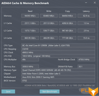
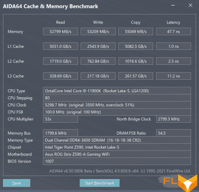
The theoretical bandwidth of the memory subsystem based on DDR5-4800 modules is 76.8 GB/s. The practically measured result almost falls into this value, which indicates the good performance of the Alder Lake memory controller when streaming data. However, the practical latency is a little frustrating. The Gear 2 controller mode, together with increased timings, makes the latency of the DDR5 memory subsystem 30% higher than when using modules of the old DDR4-3600 standard. However, Intel claims that DDR5 still delivers better performance in Alder Lake-based platforms. Whether this is really so, we will check later, when motherboards with LGA1700 and support for DDR4 SDRAM are at our disposal.
Another big change in DDR5 concerns its power supply. DDR5 SDRAM modules are equipped with their own voltage converter, which generates the required voltage of 1.1 V from the 5 V supplied from the motherboard. . True, because of this, the cost of manufacturing the DDR5 modules themselves is somewhat increased, since in addition to the chips themselves, the memory strips now also contain power elements. But fortunately, overclocking capabilities should not suffer from all these changes. Power circuits on DDR5 SDRAM modules somehow allow increasing the key voltages of DRAM VDD and DRAM VDDQ, which primarily determine the memory overclocking limits. Although, according to the specification, DDR5 memory manufacturers have the ability to both allow and prohibit changing the voltages generated by the built-in power circuit, all such restrictions are successfully bypassed by motherboards.
⇡#Intel Z690 chipset
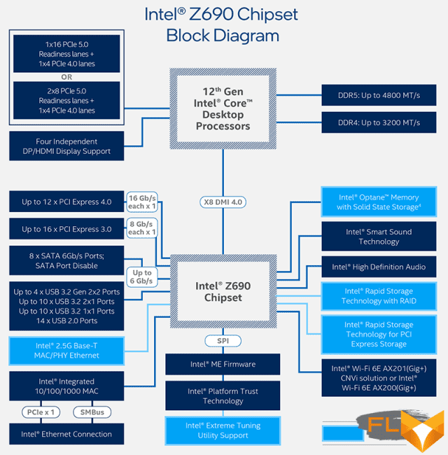
Alder Lake processors are coming to the market along with the new LGA1700 platform, which will be supported by 600-series chipsets. So far, out of many chipsets, only the first and older Z690 with overclocking functions are presented, but it is already clear from it that big changes have taken place not only in the processor direction, but in the system logic. And you can see it first of all by how this chipset communicates with the processor.
In addition to 20 PCIe lanes for the graphics card and NVMe storage, Alder Lake has a DMI 4.0 x8 bus. Representing a proprietary variant of the PCIe 4.0 x8 interface, it is responsible for the communication between the CPU and system logic. Its throughput reaches 15.76 GB / s, and this is twice the bandwidth of a bus of a similar purpose, which was used in systems based on Intel chips of the previous generation.
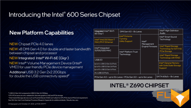
The increase in data transfer speed between the processor and the chipset is primarily due to the fact that the chipset finally has its own PCIe 4.0 lanes. Speaking specifically about the Z690, here 12 PCIe 4.0 lanes have been added to 16 PCIe 3.0 lanes. But that’s not all: the new chipset has support for up to four high-speed USB 3.2 Gen 2×2 ports with a bandwidth of 20 Gb / s, in addition to which 10 more familiar 10-Gigabit USB 3.2 Gen 2× ports have migrated from the chipsets of previous generations 1 and 10 very familiar USB 3.2 Gen 1 × 1 with a bandwidth of 5 Gb / s. The Z690 also has eight rather than six SATA ports.
Among other features of the Z690, it is also worth noting the built-in Wi-Fi 6E logic layer controller (supporting 6 GHz frequency), which can connect to physical modules using the proprietary CNVi interface. However, motherboard manufacturers are free to choose other Wi-Fi controllers that will work through PCIe.
But, speaking about the wide possibilities of the Z690, we need to make an important reservation. Do not forget that the total number of high-speed HSIO ports in the chipset is again limited, and motherboard manufacturers do not have the opportunity to implement all of the listed ports at the same time. In the case of the Z690, in particular, the port switch is designed so that the use of all 12 PCIe 4.0 chipset lines will reduce the number of available SATA ports to four.
In addition, it should be mentioned that Intel again does not offer standard tools for implementing the Thunderbolt 4 interface in LGA1700 systems. Although the corresponding block is included in the processor in mobile versions of Alder Lake, an additional controller is required in desktop configurations.
All major Intel partners have already presented their motherboards for LGA1700 – the range of announced options is estimated at several dozen models. It is noteworthy here that among the boards there are motherboards both with support for DDR5 and boards for DDR4. However, there are no combined solutions and there won’t be – this is due to the fundamentally different power supply scheme used for DDR4 and DDR5.
Also noteworthy is the fact that the Z690 chip, which is manufactured using a 14-nm process technology, does not require active cooling. On all motherboards that have been presented so far, it is cooled by passive radiators, despite the support for the high-speed PCIe 4.0 interface. This situation is different from the state of affairs in the AMD camp – there the flagship X590 chipset on most motherboards has its own cooler with a fan.
You can roughly imagine how a typical LGA 1700 motherboard based on the Z670 chipset should look like, based on the motherboard that was used in testing – ASUS ROG Strix Z690-F Gaming Wi-Fi. This board belongs to the level above the average, it is designed to work with DDR5 SDRAM, and its recommended price is set at $400. The manufacturer separately emphasizes that this solution is well suited before overclocking RAM: compatibility is declared at least with DDR5-6400 modules.
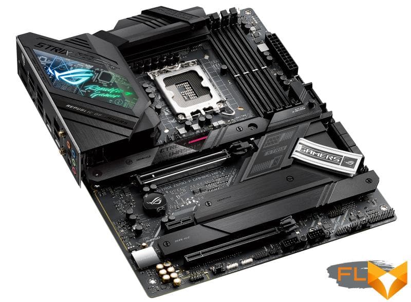
The first thing to look for when choosing boards for Alder Lake processors is the power converter. Although the new processors have become more economical than their predecessors, they can consume up to 200-300 W under serious AVX loads, which imposes certain requirements on the power supply scheme. But there are no complaints about the ROG Strix Z690-F Gaming Wi-Fi in this regard, it uses a high-quality 16 + 1-channel voltage converter, to which two eight-pin 12-V cables from the PSU are connected at once. While more powerful motherboards like the ROG Maximus Z690 Hero can carry more power phases, the ROG Strix Z690-F Gaming Wi-Fi circuitry is more than enough for even the Core i9-12900K. It uses 70-A power stages, so it is clear that under high loads, the performance of the flagship Alder Lake will not suffer.
Partly helps effective cooling VRM, which surrounds the processor socket on both sides. The radiators used in it are connected by a heat pipe and differ in rather large dimensions. However, installing massive air coolers on the ROG Strix Z690-F Gaming Wi-Fi should not be a problem. And by the way, this board allows the installation of cooling systems taken from systems of past generations – it has two sets of mounting holes that are compatible with both the new LGA 1700 and LGA 1200 coolers.
Among other things, ROG Strix Z690-F Gaming Wi-Fi brings to the user the full range of features inherent in the Z690 logic set. It offers a PCIe 5.0 x16 slot for a graphics card, 2.5 Gigabit wired networking through an Intel controller, and a rich selection of ports. The integrated sound card is based on the Realtek ALC4080 codec and the Savitech SV3H712 amplifier. The board also has a Wi-Fi 6E module. However, unlike more expensive motherboards, the ROG Strix Z690-F Gaming Wi-Fi does not have an M.2 slot that would be powered by PCIe 5.0 processor lines, which, however, can hardly be considered a disadvantage due to the lack of such drives. But there are four M.2 slots with PCIe 4.0 support on this board, and all of them have pre-installed heatsinks.
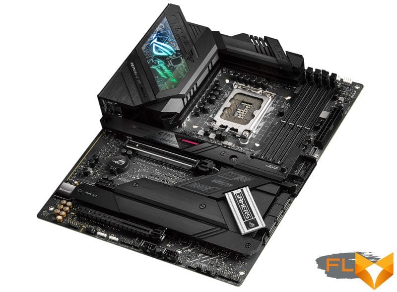
It is impossible to ignore the care of ASUS engineers about the little things, thanks to which interaction with the board becomes simply more pleasant. Examples of such chips include a button for easily removing a video card from a PCIe x16 slot; latches for M.2 slots, replacing the ever-lost screws; rear panel Clear CMOS button; BIOS Flashback technology, which allows you to update the firmware without installing a processor and memory; and a Velcro strap for routing cables in the chipset area.
⇡#New socket and form factor for LGA1700 processors
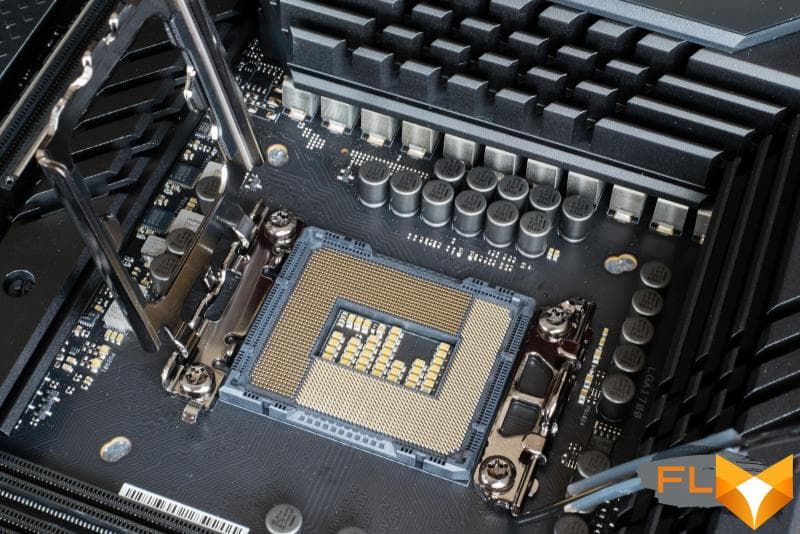
With the release of Alder Lake, a new LGA1700 processor socket comes into use. The emergence of new interfaces DDR5, PCIe 5.0 and DMI 4.0 required an increase in the number of contacts in processors, and now there are 500 more than before – 1700. Therefore, the size of the contact matrix and the dimensions of the processor socket have also increased. The LGA1700 connector has become rectangular with sides of 37.5 and 45 mm.
Along the way, Intel tried to improve the situation with the removal of heat from the processor chip. The fact is that the transition to the new Intel 7 process technology that took place in Alder Lake reduced the area of \u200b\u200bthe crystal, but due to the increase in the number of cores, it almost did not reduce its heat dissipation. This led to an increase in the heat flux density, and appropriate measures were taken to solve the problem of its removal. Intel has once again optimized the internal thermal interface, which is used under the processor cover. In Alder Lake, it’s solder again, but now the solder layer is about 15% thinner than before, which, along with a 35% reduction in the thickness of the processor die itself, should help reduce Alder Lake’s operating temperatures.
But it just didn’t work out. The reduction in die thickness and solder layer had to be compensated for by increasing the thickness of the copper processor cover, so that the processor would not be too thin and inconvenient to use. And in theory, this should also help with heat dissipation.
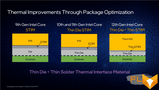
Despite the fact that the change in the thickness of the die, thermal interface and cover compensate each other in such a way that the overall height of the Alder Lake family of processors does not differ from the height of Rocket Lake, changes in the design of the LGA1700 socket itself have led to the fact that the height of the processor installed in it relative to the surface The board is still about 0.8 mm smaller than it was before. Together with the change in the area and shape of the Alder Lake processor cover, this seemed like enough reason for Intel to encourage users to make the transition to newer and more powerful cooling systems. Therefore, on LGA1700 motherboards, the holes for mounting coolers are located differently than they used to be. The distances between them have increased by a few millimeters, and the cooling systems that were used for Intel platforms of previous generations are no longer suitable for Alder Lake.
However, some cooler and motherboard manufacturers have provided various options for how to get around this problem, from placing additional mounting holes on the boards to releasing new mounts for old coolers. But, using them, users should be aware that reducing the height at which the processor cover is located above the board, one way or another reduces the pressing force of the cooling system, which may cause various problems with heat dissipation. And this means that it is still better to use specialized coolers for LGA1700 processors.
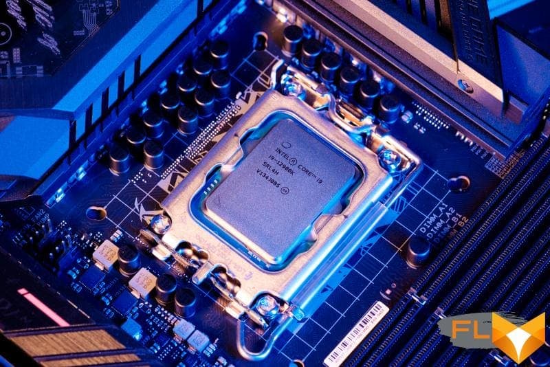
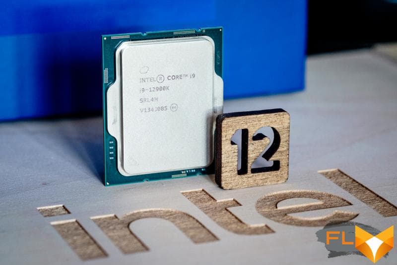
⇡#Core i9-12900K close-up
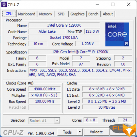
For a first look at the new generation of desktop processors, our editors received an older Alder Lake, Core i9-12900K, from Intel. This chip has 16 processing cores. Of these, eight cores are the productive Golden Cove, which operate at 4.9 GHz under full load, and in single-threaded applications overclock to 5.2 GHz. The other eight cores are energy-efficient Gracemont, their real frequency ranges from 3.7 to 3.9 GHz. Also, such a processor has a third-level cache of 30 MB, operating at a frequency of 3.6 GHz, which is limited by the frequency of E-cores.
Even though the E-cores run at a low frequency, their contribution to the overall performance of the Core i9-12900K can be quite noticeable. At the very least, the inclusion of eight additional E-cores increases performance more than Hyper-Threading support for eight P-cores. You can verify this by the graph below of the dependence of the result of Cinebench R23 on the number of threads involved.
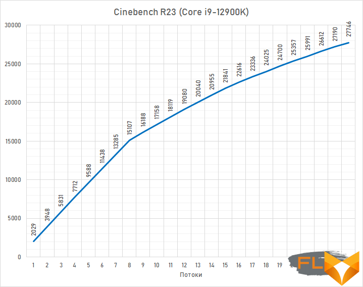
There are two inflection points on the above curve. Their nature becomes clear if we recall that, having equal threads, the Windows scheduler first loads P-cores (one thread per core), then E-cores, and only then virtual cores created on the basis of P-cores by Hyper-Threading technology . If we summarize the indicators from the graph, it turns out that the average contribution to the performance of the P-core without Hyper-Threading technology is approximately 1890 points, and the execution of the second thread on the same cores adds an average of 640 points. The contribution made to the overall result of Cinebench R23 by each E-core is plus or minus 940 points. In other words, single-threaded E-core performance at 3.7GHz can be estimated at half the single-threaded performance of P-core at 4.9GHz, which is pretty good.
Thus, E-cores in Alder Lake are by no means an unnecessary component, and processor models with fewer of them will indeed have worse performance in multi-threaded tasks. However, there are cases when E-cores are still better off. This can help for better overclocking of the processor, for increasing the frequency of its L3 cache, or in case the P-cores need to return the AVX-512 functionality that is blocked by the E-cores.
Judging by the recommended price, Intel wants the Core i9-12900K to be seen as a rival to the 12-core Ryzen 9 5900X, and this has its own logic. These processors are capable of running the same number of threads – 24. True, the Core i9-12900K has an advantage in the total number of cores, but the Ryzen 9 5900X wins in the number of large productive cores.
| Ryzen 9 5950X | Core i9-12900K | Ryzen 9 5900X | Core i9-11900K | |
|---|---|---|---|---|
| Kernels | 16 | 8P+8E | 12 | 8 |
| Threads | 32 | 24 | 24 | 16 |
| P-core frequencies, GHz | 3.4-4.9 | 3.2-5.2 | 3.7-4.8 | 3.5-5.3 |
| E-core frequencies, GHz | – | 2.4-3.9 | – | – |
| TDP/PBP, W | 105 | 125 | 105 | 125 |
| MTP, Tue | 142 | 241 | 142 | – |
| L3 cache, MB | 2 × 32 | 30 | 2 × 32 | 16 |
| Memory | DDR4-3200 | DDR4-3200 DDR5-4800 | DDR4-3200 | DDR4-3200 |
| Integrated graphics | No | UHD 770 | No | UHD 760 |
| PCIe | 24 lines 4.0 | 16 lines 5.0 | ||
| 4 lines 4.0 | 24 lines 4.0 | 20 lines 4.0 | ||
| Price | $799 | $589 | $549 | $549 |
The Core i9-12900K is priced at $40 more than its 12-core competitor, perhaps in this way the manufacturer wants to point out other advantages of its product – support for DDR5 memory and PCIe 5.0 interface. Plus, Intel processors currently look more advantageous due to the fact that they have some kind of integrated graphics. However, it is also impossible to say that the Ryzen 9 5900X definitely loses in terms of performance. On the AMD supply side, there is a larger cache memory and formally better economy.
The MTP consumption limit for the entire 16-core Core i9-12900K is set by the specification at 241 W, but in reality its maximum consumption in resource-intensive applications like Blender or Cinebench R23 fits into 210-215 W. And this means that the Core i9-12900K is more economical than the older representatives of the Rocket Lake and Comet Lake families, despite the significant superiority in the number of cores.
All this is confirmed by practical checks of consumption and temperature. If we talk about a multi-threaded resource-intensive load (our test used rendering in Cinebench R23), then the Core i9-12900K is significantly more economical than its predecessor in the face of the Core i9-11900K, but still exceeds the competing Ryzen 9 5900X in terms of consumption.
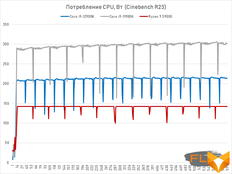
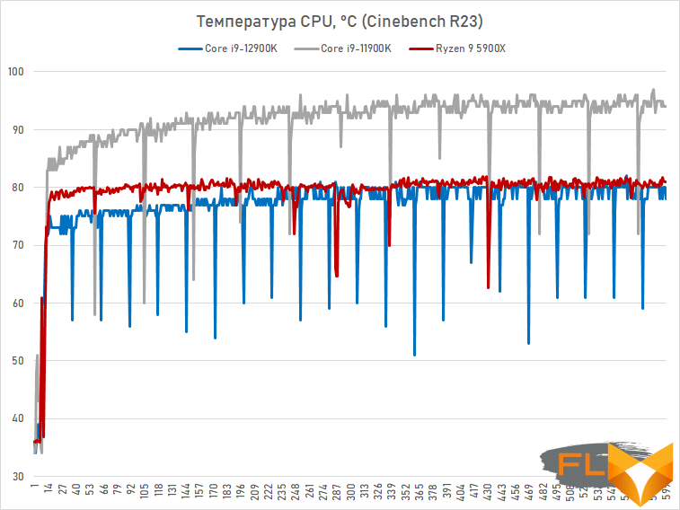
However, if we talk about temperatures, which are determined not only by the heat dissipation of processors, but also by how efficiently a particular processor allows it to be removed, then the Core i9-12900K is in the lead. When testing the Core i9-12900K, Core i9-11900K and Ryzen 9 5900X with the same liquid cooling system (in this case it is a custom circuit on EKWB components with a 360 mm radiator), it turns out that with the same resource-intensive load, the older Alder Lake heats up averaging up to 78 degrees, while the Ryzen 9 5900X averages 80 degrees. And compared to the Core i9-11900K, the new Core i9-12900K seems like an alien from another world: despite twice the number of cores, the temperature to which it heats up is 15 degrees lower.
An even more interesting situation can be seen in the game application. Here, all the cores available in the processors are not used, thanks to which the Thread Director technology can show itself in all its glory. All game threads do not need to be executed on productive cores, and some of them are redirected to E-cores, which makes the Core i9-12900K phenomenally economical – its practical consumption is a couple of tens of watts lower than that of the Ryzen 9 5900X. Comparing the consumption of Core i9-12900K and Core i9-11900K does not make any sense at all – these two processors look like representatives of completely different worlds in the graph below.
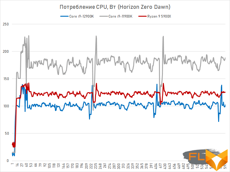
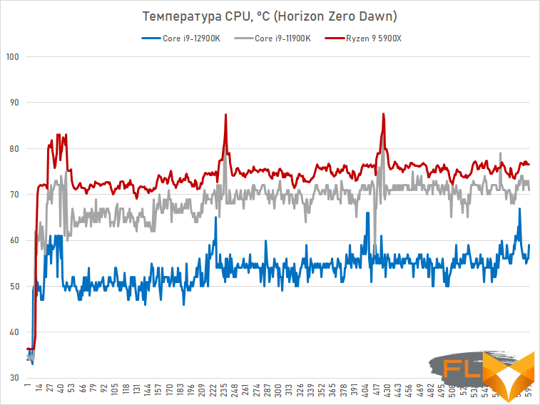
This power consumption situation translates into much lower temperatures for the Core i9-12900K. In a gaming load, this processor does not get above 55-60 degrees, which allows it to stay about 15-17 degrees cooler than the Core i9-11900K, and 20 degrees cooler than the Ryzen 9 5900X.
Obviously, the measures taken by Intel to facilitate heat dissipation from the processor chip were not in vain. Under real load, the temperatures of the Core i9-12900K are lower than other flagship offerings, and at times significantly. But keep in mind that this is not due to moderate heat release, but to the relative ease of removing heat from the processor chip. In other words, the flagship Alder Lake will seem like a cold processor only when using a sufficiently effective cooling system. At the same time, at peak loads, it is capable of a fairly high heat dissipation – more than 200 watts, and this is noticeably higher than the heat dissipation of any of the AMD processors.
⇡#Overclocking
The latest generation processors leave almost no room for overclocking, if we talk about it not as a sports discipline, but as a way to get extra performance for everyday use. Alder Lake processors are no exception here, especially if we consider the older model Core i9-12900K – its frequencies are brought to values close to the maximum already by the manufacturer.
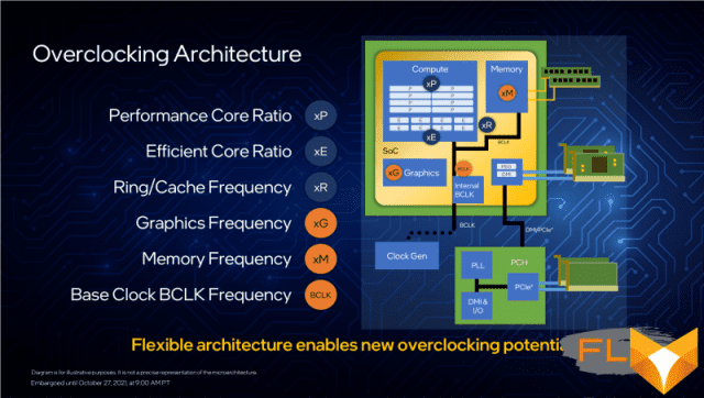
Nevertheless, Intel continues to implement numerous overclocking features in its CPUs. So, all six Alder Lake models released today have free multipliers, which makes them great objects for all sorts of experiments. In this sense, the new processors are even more interesting than their predecessors, since they have two types of cores at once, operating at different frequencies. Accordingly, these cores use different multipliers and are overclocked separately. True, they are still powered by a single voltage.
If we talk about overclocking limits, then the P-cores of the processor instance at our disposal were overclocked to 5.1 GHz, and the E-cores to 3.9 GHz. In this state, he managed to pass stability tests with the condition of additional frequency reduction when executing AVX instructions at 100 MHz. By the way, the delta clock frequency for AVX instructions set via the BIOS of the motherboard affects only the P-cores, so the frequencies of the test Core i9-12900K on the AVX load were 5.0 / 3.9 GHz.
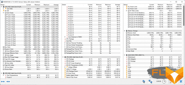
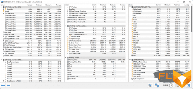
Voltage for such acceleration had to be adjusted minimally. The settings used included setting Load-Line Calibration to Level 4 and a symbolic increase in CPU voltage of 0.01 V via Offset.
The stability of the overclocked processor was tested in Prime95, and its temperatures under such a load exceeded 90 degrees. But thanks to a custom liquid cooling system, throttling, which Alder Lake turns on at 100 degrees, was avoided. The actual voltage on the processor, which was observed during the stress test, was 1.215 V at AVX2- and 1.25 V at normal load.
In addition to freely changing multipliers, Alder Lake processors allow you to disable their cores with the only condition – in the end, at least one P-core must remain active. This can be used for overclocking. As practice has shown, when the E-cores are turned off, the P-cores open up additional frequency potential. And this property of Alder Lake is quite possible to use. In particular, if a computer based on this processor is mainly used for games that cannot use all 16 cores of the Core i9-12900K, disabling E-cores will most likely not reduce its performance, and additional overclocking of P-cores will play a positive role.
However, it is still not worth counting on a noticeable increase in frequency. For example, the frequency of our copy of the Core i9-12900K, after turning off its E-cores, was increased by only 100 MHz – up to 5.2 GHz.
As you can see, disabling the E-cores reduces the power consumption of Alder Lake by about 50W, but this does not lead to any significant change in the overclocking limits. The temperature regime also changes little – it is possible to win back only a couple of degrees.
⇡#Description of the test system and testing methodology
Unfortunately, Intel provided us with the equipment we needed to get acquainted with Alder Lake much later than we would like. Therefore, in the first review of the Core i9-12900K, we will not be able to pay attention to all aspects of performance. However, a little later we will certainly catch up. In the same material, we will talk about comparing the performance of the Core i9-12900K, equipped with DDR5 memory, with the performance of other flagship processors on the market, performed in the Windows 11 operating system. The main rivals of the older Alder Lake will be the 12-core Ryzen 9 5900X and The 8-core Core i9-11900K, but on the charts you can find the results of other Ryzen 9 and Core i9 processor families released since the summer of 2019.
The test system included the following components:
- Processors:
- AMD Ryzen 9 5950X (Vermeer, 16 cores + SMT, 3.4-4.9GHz, 64MB L3);
- AMD Ryzen 9 5900X (Vermeer, 12 cores + SMT, 3.7-4.8GHz, 64MB L3);
- AMD Ryzen 9 3950X (Matisse, 12 cores + SMT, 3.5-4.7GHz, 64MB L3);
- AMD Ryzen 9 3900XT (Matisse, 12 cores + SMT, 3.8-4.7GHz, 64MB L3);
- Intel Core i9-12900K (Alder Lake, 8P+8E-cores + HT, 3.5-5.3/2.4-3.9GHz, 30MB L3);
- Intel Core i9-11900K (Rocket Lake, 8 cores + HT, 3.5-5.3GHz, 16MB L3);
- Intel Core i9-10900K (Comet Lake, 10 cores + HT, 3.7-5.3GHz, 20MB L3).
- CPU cooler: EKWB custom coolant
- Motherboards:
- ASUS ROG Crosshair VIII Hero (Socket AM4, AMD X570);
- ASUS ROG Strix Z590-A Gaming WiFi (LGA1200, Intel Z590);
- ASUS ROG Strix Z690-F Gaming WiFi (LGA1700, Intel Z690).
- Memory:
- 2x16GB DDR4-3600 SDRAM, 16-18-18-38 (Crucial Ballistix RGB BL2K16G36C16U4BL);
- 2 × 16 GB DDR5-4800 SDRAM, 38-38-38-70 (Kingston Fury Beast KF548C38BBK2-32).
- Video Card: NVIDIA GeForce RTX 3090 Founders Edition (GA102, 1395-1695/19500MHz, 24GB GDDR6X 384-bit).
- Disk subsystem: Intel SSD 760p 2TB (SSDPEKKW020T8X1).
- Power supply: Thermaltake Toughpower DPS G RGB 1000W Titanium (80 Plus Titanium, 1000W).
All compared processors were tested with the settings accepted by the board manufacturers by default. This means that for Intel platforms, the TDP/PBP limits specified in the specifications are ignored, and instead the maximum possible frequencies are used in order to obtain maximum performance. The vast majority of users operate processors in this mode, since enabling heat dissipation and power consumption limits in most cases requires special BIOS settings.
Memory subsystem settings for all systems were performed using XMP profiles. This means that LGA1200 and Socket AM4 processors were tested with DDR4-3600, while Alder Lake was tested with DDR5-4800.
Testing was performed on the Microsoft Windows 11 Pro (21H2) Build 22000.282.0 operating system with KB5005635 and KB5006746 updates installed and using the following driver set:
- AMD Chipset Driver 3.10.08.506;
- Intel Chipset Driver 10.1.18838.8284;
- Intel SerialIO Driver 30.100.2105.7;
- Intel Management Engine Interface 2124.100.0.1096;
- NVIDIA GeForce 496.49 Driver
Description of the tools used to measure computing performance:
Comprehensive benchmarks:
- Futuremark PCMark 10 Professional Edition 2.1.2508 – testing in Essentials scenarios (typical work of the average user: launching applications, surfing the Internet, video conferencing), Productivity (office work with a word processor and spreadsheets), Digital Content Creation (creating a digital content: photo editing, non-linear video editing, rendering and visualization of 3D models).
- 3DMark Professional Edition 2.17.7173 – testing in Time Spy Extreme 1.0 scene.
Applications:
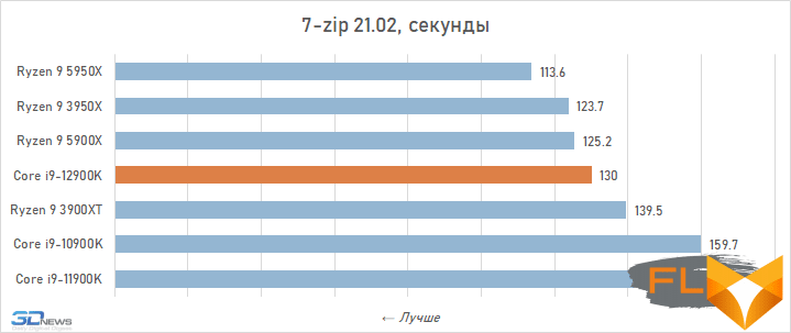
- 7-zip 21.02 – archiving speed testing. The time taken by the archiver to compress a directory with various files with a total volume of 3.1 GB is measured. Uses LZMA2 algorithm and maximum compression ratio.
- Adobe After Effects 2021 18.4.0 – Animation Render Speed Test. The time taken by the system to render a pre-prepared video in 1920 × 1080@30fps resolution is measured.
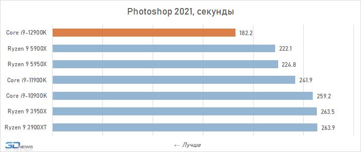
- Adobe Photoshop 2021 22.4.3 – Graphics performance testing. The average execution time of the Puget Systems Adobe Photoshop CC Benchmark 18.10 test script, which simulates the typical processing of an image taken by a digital camera, is measured.
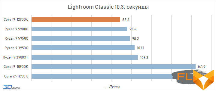
- Adobe Photoshop Lightroom Classic 10.3 – Performance test for batch processing of a series of RAW images. The test scenario includes post-processing and export to JPEG at a resolution of 1920 × 1080 and a maximum quality of two hundred 16-megapixel RAW images taken with a Fujifilm X-T1 digital camera.
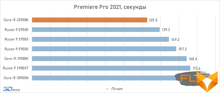
- Adobe Premiere Pro 2021 15.4.0 – performance testing for non-linear video editing. This measures the rendering time to YouTube 4K for a project containing HDV 2160p30 footage with various effects applied.
- Blender 2.93.5 – testing the speed of the final rendering in one of the popular free packages for creating three-dimensional graphics. The duration of building the final model pavillon_barcelona_v1.2 from Blender Benchmark is measured.
- Cinebench R23 is the standard benchmark for testing rendering speed in Cinema 4D R23.
- Magix Vegas Pro 19.0 – performance testing for non-linear video editing. This measures the rendering time to YouTube 4K for a project containing HDV 2160p30 footage with various effects applied.
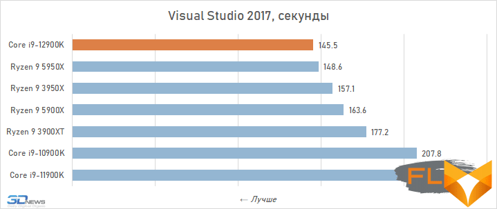
- Microsoft Visual Studio 2017 (15.9.40) – Compile time measurement for a large MSVC project – Blender 2.79b professional 3D package.
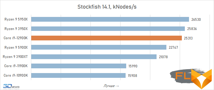
- Stockfish 14.1 – testing the speed of the popular chess engine. The speed of enumeration of options in the position “1q6/1r2k1p1/4pp1p/1P1b1P2/3Q4/7P/4B1P1/2R3K1 w” is measured.
- SVT-AV1 v0.8.6 – testing the speed of video transcoding into the promising AV1 format. Performance is measured using a raw 1080p@50FPS AVC video file with a bitrate of about 30 Mbps.
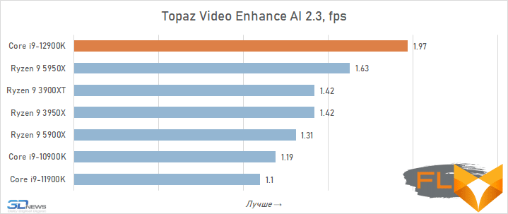
- Topaz Video Enhance AI v2.3.0 – performance testing in an AI-based program to improve video detail. The test uses the original video at 640×360 resolution, which is doubled using the Artemis Anti Aliasing v9 model.
- V-Ray 5.00 – Benchmark the performance of a popular rendering system using the standard V-Ray Benchmark Next application.
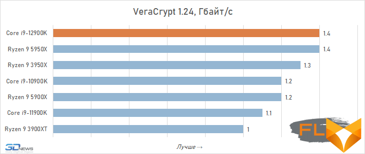
- VeraCrypt 1.24 – cryptographic performance testing. The benchmark built into the program is used, which uses Kuznyechik-Serpent-Camellia triple encryption.
- x264 r3059 – testing the speed of transcoding video to H.264/AVC format. To evaluate performance, we use the original 2160p@24FPS AVC video file with a bitrate of about 42 Mbps.
- x265 3.5+8 10bpp – testing the speed of video transcoding to H.265/HEVC format. To evaluate performance, we use the original 2160p@24FPS AVC video file with a bitrate of about 42 Mbps.
Games:
- Assassin’s Creed Valhalla. Resolution 1920 × 1080: Graphics Quality = Very High. Resolution 3840 × 2160: Graphics Quality = Very High.
- Borderlands 3. Resolution 1920 × 1080: Graphics API = DirectX 12, Overall Quality = Badass. Resolution 3840 × 2160: Graphics API = DirectX 12, Overall Quality = Badass.
- Chernobylite. Resolution 1920 × 1080: Graphics Quality = Ultra. Resolution 3840 × 2160: Graphics Quality = Ultra.
- Civilization VI: Gathering Storm. Resolution 1920×1080: DirectX 12, MSAA=4x, Performance Impact=Ultra, Memory Impact=Ultra. Resolution 3840 × 2160: DirectX 12, MSAA = 4x, Performance Impact = Ultra, Memory Impact = Ultra.
- Cyberpunk 2077. 1920×1080 resolution: Quick Preset = Ray Tracing – Ultra. Resolution 3840 × 2160: Quick Preset = Ray Tracing – Ultra.
- Far Cry 6. Resolution 1920 × 1080: Graphics Quality = Ultra, HD Textures = On, Anti-Aliasing = TAA. Resolution 3840 × 2160: Graphics Quality = Ultra, Anti-Aliasing = TAA.
- Hitman 3. 1920 × 1080 resolution: Super Sampling = 1.0, Level of Detail = Ultra, Texture Quality = High, Texture Filter = Anisotropic 16x, SSAO = Ultra, Shadow Quality = Ultra, Mirrors Reflection Quality = High, SSR Quality = High, Variable Rate Shading = Quality. Resolution 3840 × 2160: Super Sampling = 1.0, Level of Detail = Ultra, Texture Quality = High, Texture Filter = Anisotropic 16x, SSAO = Ultra, Shadow Quality = Ultra, Mirrors Reflection Quality = High, SSR Quality = High, Variable Rate Shading =Quality.
- Horizon Zero Dawn. Resolution 1920 × 1080: Preset = Ultimate Quality. Resolution 3840 × 2160: Preset = Ultimate Quality.
- Metro Exodus Enhanced. Resolution 1920 × 1080: Shading Quality = Ultra, Ray Tracing == Normal, Reflection = Raytraced, Variable Rate Shading = 4x, Hairworks = Off, Advanced PhysX = Off, Tesselation = Off. Resolution 3840 × 2160: Shading Quality = Ultra, Ray Tracing == Normal, Reflection = Raytraced, Variable Rate Shading = 4x, Hairworks = Off, Advanced PhysX = Off, Tesselation = Off.
- Shadow of the Tomb Raider. Resolution 1920×1080: DirectX12, Preset=Highest, Anti-Aliasing=TAA. Resolution 3840 × 2160: DirectX12, Preset = Highest, Anti-Aliasing = Off.
- A Total War Saga: Troy. Resolution 1920 × 1080: DirectX 12, Quality = Ultra, Unit Size = Extreme. Resolution 3840 × 2160: DirectX 12, Quality = Ultra, Unit Size = Extreme.
- Watch Dogs Legion. Resolution 1920×1080: DirectX 12, Quality=Ultra, RTX=Off, DLSS=Off. Resolution 3840 × 2160: DirectX 12, DirectX 12, Quality = Ultra, RTX = Off, DLSS = Off.
In all gaming tests, the results are the average number of frames per second, as well as the 0.01-quantile (first percentile) for FPS values. The use of the 0.01-quantile instead of the minimum FPS is due to the desire to clean up the results from random bursts of performance that were provoked by reasons not directly related to the operation of the main components of the platform.
⇡#Performance in complex benchmarks
The comprehensive PCMark 10 test, which assesses the performance of systems during normal everyday work, puts the new Core i9-12900K in first place in all three scenarios included in it. We will not undertake to claim that this victory immediately indicates the highest performance of the new product, since the results of PCMark 10 have some specifics associated with its use for measuring low-threaded office applications. But on the other hand, we can say with full confidence that the Thread Director technology in Windows 11 at least does not spoil anything. The first two office scenarios from PCMark 10 are partially executed on E-cores, but this does not lead to any noticeable decrease in performance. In other words, during normal user activity, the Core i9-12900K shows a good level of performance and, importantly, high responsiveness of foreground tasks.
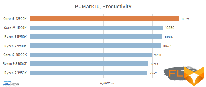

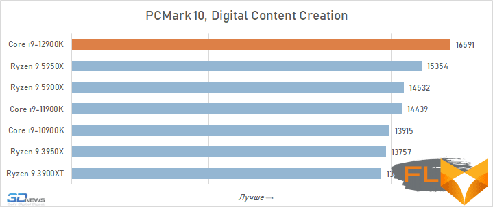
The third scenario in this comprehensive benchmark (Digital Content Creation) is dedicated to working with digital content, but the performance of the Core i9-12900K also looks very convincing in it. Given this result, Alder Lake can be expected to outperform 12- and 16-core processors based on the Zen 3 microarchitecture in a wide range of resource-intensive tasks, and this will be tested below.
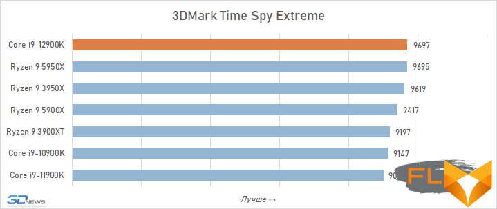
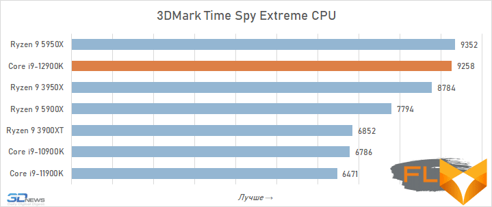
At the same time, in the 3DMark Time Spy gaming benchmark, the new Core i9-12900K scores slightly less processor points compared to the Ryzen 9 5950X. However, the 16-core AMD costs significantly more. The simpler 12-core Ryzen 9 5900X, which is close in price to the Core i9-12900K, is noticeably behind the new Intel.
⇡#Performance in Applications
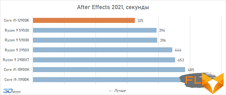
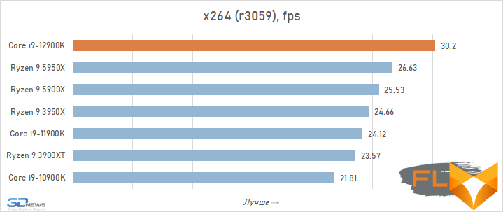
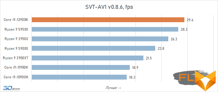
But commenting on the results obtained in resource-intensive applications, we can already say for sure: Alder Lake was a success. The increase in the number of cores, the transition to a more advanced microarchitecture, the growth of cache memory and the use of faster DDR5 memory in total give a very noticeable effect. Compared to the Core i9-11900K, the new Core i9-12900K is on average almost one and a half times faster. Moreover, even in the most unfavorable cases, the new processor shows at least a 25 percent advantage over its predecessor.
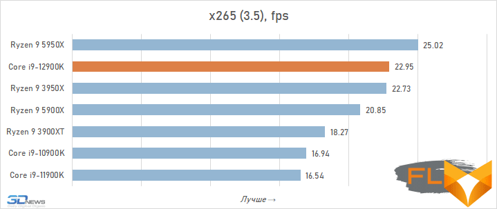
The older Alder Lake does not hit the face in the dirt even if its performance is compared with the performance of AMD’s current top-level offerings. In all tests, with the exception of the archiver, the Core i9-12900K is noticeably faster than the competing 12-core Ryzen 9 5900X, and, moreover, the Core i9-12900K boasts generally higher performance, including against the background of a 16-core processor with microarchitecture Zen 3. The average superiority of the flagship Alder Lake over the Ryzen 9 5900X reaches 18%, and over the Ryzen 9 5950X – 6%. But at the same time, we need to make a reservation that the current 16-core AMD still manages to defend its primacy in four tasks out of 16. Among these tasks is the already mentioned 7-zip archiver, in which a capacious cache helps the AMD processor, as well as x265, Stockfish and V-Ray, which actively use AVX2 instructions in their work.
Nevertheless, the conclusion is clear. The Ryzen 9 5950X no longer holds the title of best processor for work. Intel now has a more attractive solution that also costs significantly less.
Rendering:
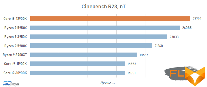
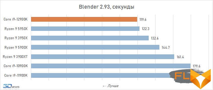
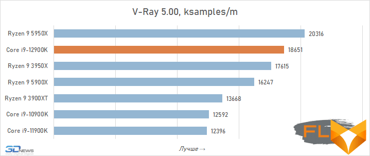
Photo processing:
Video work:

Video transcoding:
Compilation:
Archiving:
Chess:
Encryption:
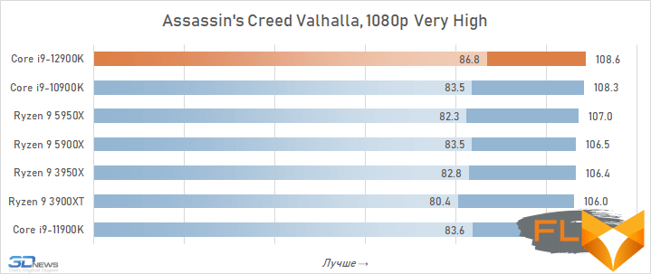
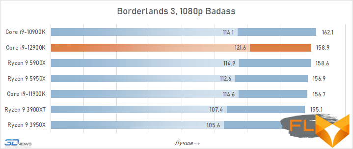
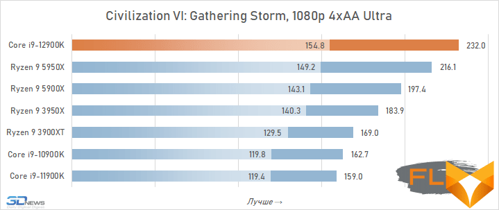
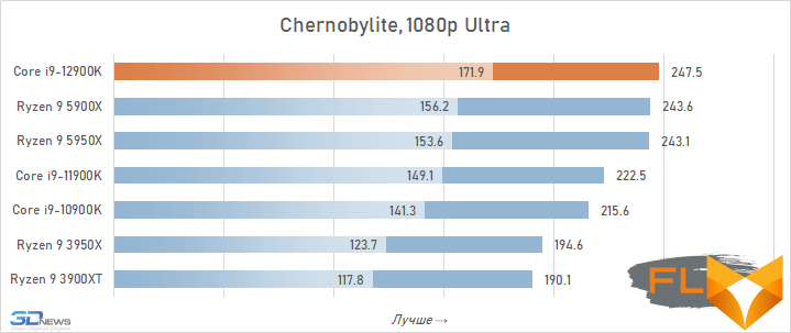
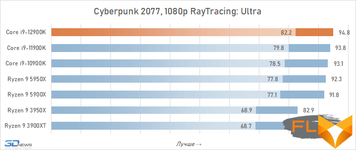
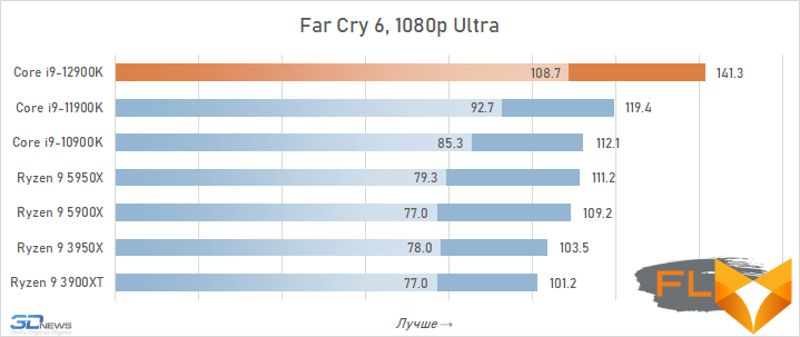
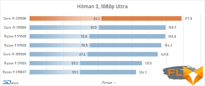
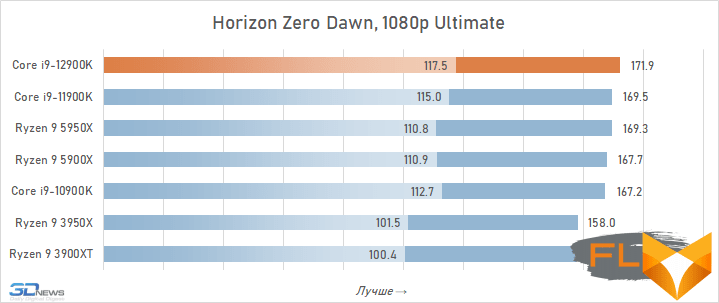
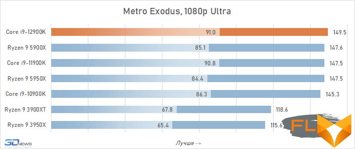
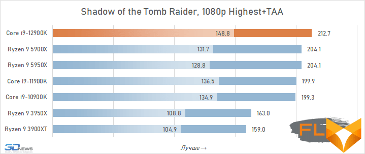
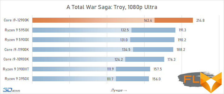
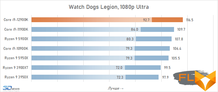
⇡#1080p gaming performance
The performance of Intel processors in gaming applications has never been satisfactory. And belonging to the previous generation of Rocket Lake, in some cases, it turned out to be an even more preferable option for the basis of gaming systems compared to AMD Ryzen processors. However, the arrival of the family, Alder Lake and the Core i9-12900K in particular, destroys all gaming parity between AMD and Intel offerings that has existed to date. All disputes about which processor deserves the title of the best CPU for games will now have to be stopped – the new Core i9-12900K is clearly more productive than any other options. To see this, just look at the graph of the average frame rate, built according to the results of tests in 12 titles in Full HD using the GeForce RTX 3090 graphics accelerator. In terms of average frame rate, the Core i9-12900K is 10% faster than the Core i9-11900K , and 7-9% than Ryzen 9 5950X and Ryzen 9 5900X. There is also a commensurate advantage in the minimum FPS, it reaches 10 and 13%, respectively.

The charts below show how the performance of the Core i9-12900K varies from game to game. However, we did not see a single case where the Core i9-12900K would be inferior to some other processor by an amount exceeding the measurement error. But the level of its separation from the nearest competitors can in some cases exceed both 10 and 15%.
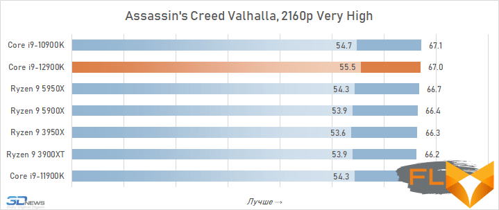
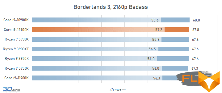
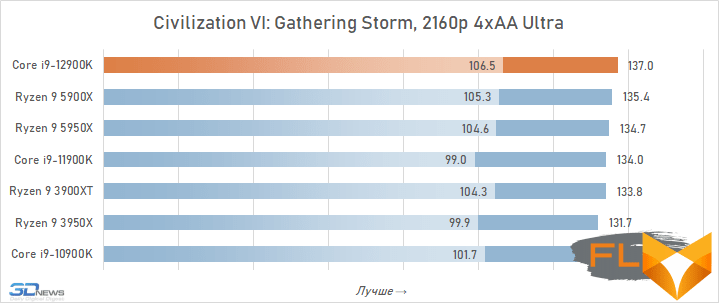
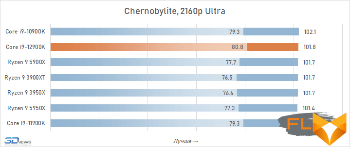
⇡#Gaming performance at 2160p
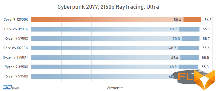
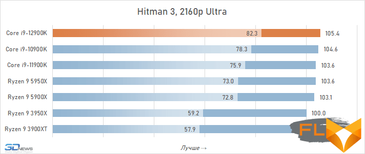
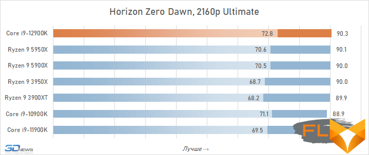
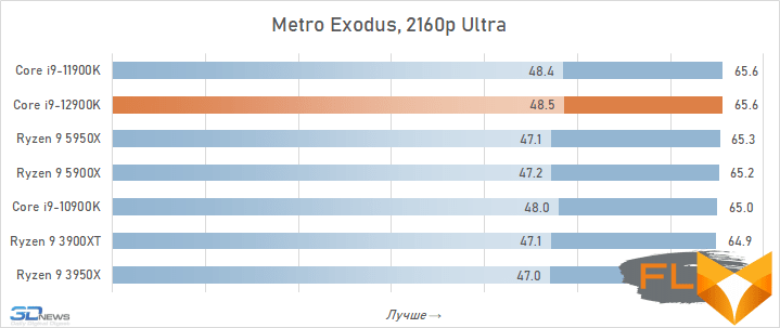
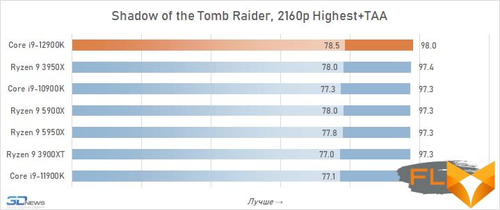
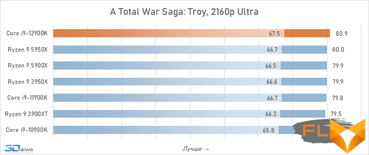
The graphics of modern games are gradually becoming more and more complex, and in 4K resolution everything is gradually moving towards redistributing the load in favor of the video card. Therefore, the further, the less impact on the frame rate at this resolution has the CPU, even if the system has the fastest gaming graphics card in existence. In other words, don’t be surprised that even a processor as powerful as the Core i9-12900K doesn’t break away from its rivals in the graphs below. But in some situations, the advantage of the older Alder Lake still manifests itself and it turns out to be 1-2% faster than the alternatives.


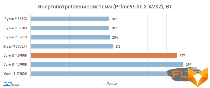
⇡#Energy Consumption
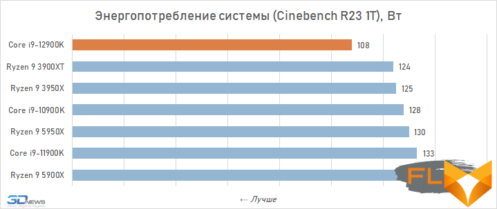
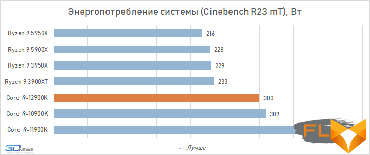
With a preliminary acquaintance with the Core i9-12900K, we have already seen that this processor has become less voracious compared to its predecessors, despite the fact that we are talking about a much more complex chip. But the new Intel 7 manufacturing technology, which has not yet been used in desktop processors or any other, has helped make Alder Lake a more cost-effective solution. However, this is partly due to the “low base effect”, since the same Rocket Lake power consumption reached a very indecent level. And if the consumption of the Core i9-12900K is compared with the consumption of current AMD offers, then there is no need to talk about any cost-effectiveness of the new product. Here, Intel still loses a lot to its competitor.
The results of measurements of the total consumption of systems (without monitors) given below allow you to visually verify the above. But there is an important nuance: high consumption is characteristic of the Core i9-12900K only with a multi-threaded resource-intensive load. If we are talking about a single-threaded load, then the picture changes to the opposite. In such a situation, Alder Lake is distinguished by rather modest appetites compared to other modern processors.
⇡#Conclusions
More recently, it seemed that processors based on the Zen 3 architecture are so good that nothing threatens their dominance. Especially in work tasks, which they easily deal with thanks to the chiplet design, a large number of powerful computing cores and a capacious cache memory. However, today it turned out that the flagship 16-core Ryzen 9 5950X is no longer the leader, because the Intel Alder Lake processor family has entered the market. And this is simply amazing, because no one imagined that the new Intel development could be so good. The eldest representative in the Alder Lake family, the Core i9-12900K, has only eight productive cores and can only execute 24 threads, but this does not prevent it from outperforming the competitor’s 16-core and 32-thread processor in most tasks. What’s more, the official price of the Core i9-12900K is a quarter of the price of the Ryzen 9 5950X, making the new Intel processor an absolutely incredible value proposition.
It looks like something has changed drastically inside Intel. Either the “magic kick” from AMD acted this way, or the changes in the company’s management team affected, but Alder Lake really recognizes that old Intel of the middle and end of the “zero” years, when Conroe, Yorkfield processors entered the market one after another , Lynnfield and Sandy Bridge. As then, at Alder Lake, the company clearly did not skimp on innovation. These processors received a very large array of multidirectional improvements, including reworking the microarchitecture and a serious increase in IPC, an increase in the number of computing cores, the introduction of a hybrid architecture and Thread Director technology, a transition to a new manufacturing process and the emergence of support for faster types of memory. Previously, even one of these changes could have been a very noticeable event for Intel processors, but now the entire list has fired in one salvo, and this has a very impressive effect.
During the event dedicated to the announcement of the Core i9-12900K, this CPU was named the best processor in the world for games, and this was not an exaggeration. Testing has confirmed that the older Alder Lake is indeed noticeably superior in gaming performance to both all members of the Ryzen 5000 family, as well as processors from the Comet Lake and Rocket Lake generations. If we use Full HD resolution as a guideline, then the advantage of the novelty in some cases can be a double-digit percentage. At the same time, the Core i9-12900K does not lose its face in applications for creating and processing digital content. In many heavy resource-intensive tasks for professional work, it is faster than the 16-core Ryzen 9 5950X, and often the magnitude of its advantage is not lower than in games.
As a result, the shortcomings of the Core i9-12900K can only be attributed to a rather high heat dissipation under serious loads, but in fairness it should be noted that Intel has done everything possible so that this chip does not overheat during operation. At least, it is relatively easy to remove heat from it, you only need a high-quality cooling system.
So far, we have only met the senior representative of the Alder Lake family, but the models of the Core i7 and Core i5 series related to it will almost certainly be no worse in their weight categories. This directly follows from their characteristics, since cheaper modifications in the family differ from the older processor not so dramatically. Therefore, it is quite clear that serious changes will begin to occur in the desktop processor market in the near future. AMD will have to aggressively cut the prices of its offerings, and Intel will have to try to meet the demand for Alder Lake processors, which is sure to be considerable.
Most Popular Articles
Find the Best DDR3 RAM For Gaming Overclocking
Review laptop ASUS ROG Flow X13 (GV301QH-K5228T): what progress has come!

Best Motherboard for the Amd Ryzen 9 5900x in 2024
Laptops with sim card slot – Best laptop with a sim card slot in 2024 lte
How to Remove Hard Drive from Laptop
AMD Ryzen 5 5500 Processor Review: An Affordable Six-Core That Was Too Late